3D Solder Paste Inspection
Measure the height, area and true volume of every paste deposit before a single component is placed, with systems we design and manufacture ourselves.
Solder paste printing is the first process step in surface-mount assembly, and it is widely regarded as the largest single source of solder-joint defects. A deposit that is too low, too small, offset or bridged looks fine to the eye and then becomes an open, a short or a weak joint after reflow, when it is far more expensive to find and fix.
Solder paste inspection measures each deposit in three dimensions straight after printing. Boards that are out of limits are wiped and reprinted for pennies, and the measurement data tells you when the printer is drifting before it starts making defects.
VisionMaster has built SPI systems since the 1990s. Every system we sell is designed, built and supported by the same engineering team, from the optics and sensor head to the measurement software.
What SPI measures
Height
Deposit height against the stencil thickness, the earliest indicator of stencil, squeegee and paste problems.
True volume
Actual paste volume per pad from a full 3D profile, the measurement that best predicts joint quality.
Area
Printed area as a percentage of the aperture, to catch insufficient and excessive prints.
Offset
Print registration against the pad, so misalignment is corrected before it causes bridging or tombstoning.
Bridging
Paste connecting adjacent pads on fine-pitch parts, caught before it becomes a short.
Process trends
Built-in SPC charting shows drift over time, so you adjust the process instead of sorting bad boards.
How our SPI systems work
Structured light projection
A pattern of white or infrared light is projected onto the board. The pattern deforms over every paste deposit in proportion to its height.
3D reconstruction
A high-resolution camera captures the deformed pattern and the software reconstructs a complete height map of the field of view.
Automatic measurement
Deposits are found automatically and measured for height, area and volume against the limits you set. No manual cursor placement and no operator judgement.
Data and SPC
Results are charted in real time and stored, giving you the evidence to tune the print process and to show customers and auditors.
Systems We Build
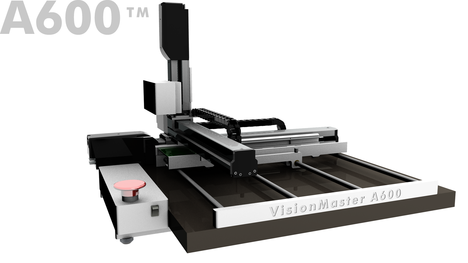
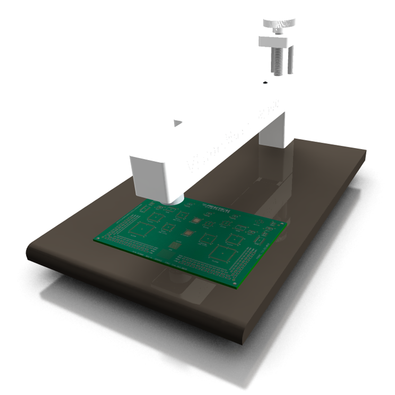
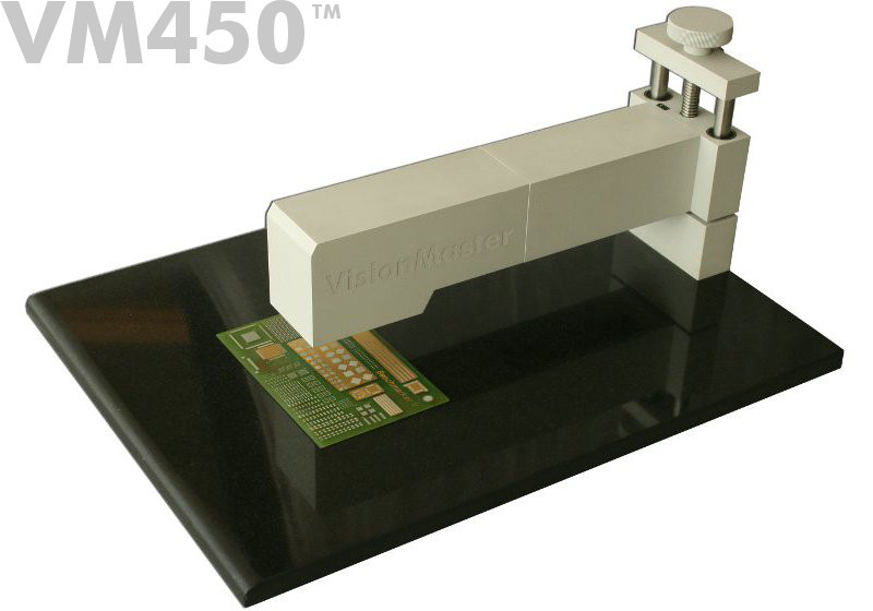
Frequently Asked Questions
What is solder paste inspection (SPI)?
SPI is the automated 3D measurement of solder paste deposits on a PCB after printing and before component placement. It measures the height, area and volume of each deposit so that print defects are caught while they are still cheap to correct.
Do I need 3D SPI or is 2D enough?
2D inspection sees area and position only. Paste volume, which depends on height, is the variable most closely tied to solder joint quality, and it can only be measured in 3D.
Should I choose a benchtop or a fully automatic system?
A benchtop system suits process setup, sampling and low to medium volumes where an operator checks critical pads. A fully automatic system inspects whole boards unattended and suits higher volumes or products that need every board measured.
How do I justify the cost of SPI?
The usual justification is reduced rework and scrap. Our ROI calculator lets you enter your own volumes, defect rates and costs to estimate annual savings and payback.
Discuss Your Application
Send us a description of the part and what you need to detect or measure. An engineer will reply, not a sales script.